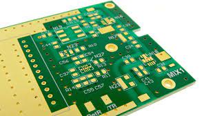
RF Circuit Boards for Low Noise Operation
RF and microwave signals are very sensitive to noise, ringing, reflections and other intrusions that can significantly reduce performance and reliability. As a result, RF circuit boards require special design considerations to ensure their proper operation. These steps include careful selection of substrate materials, proper use of decoupling capacitors and impedance-matching techniques, efficient thermal management and the use of ground planes.
When selecting a substrate for an RF circuit board, it is important to choose a material with a low loss tangent and CTE (Coefficient of Thermal Expansion). Polytetrafluoroethylene (PTFE) and ceramics are excellent choices because they have low losses, high dielectric constants and good thermal conductivity.
The material also must be stable to minimize changes in dielectric properties due to the presence of copper traces and other components. To ensure a high degree of stability, rf circuit board are often constructed using a multilayer construction with multiple dielectric layers between conductive layer metals.
RF circuit boards must incorporate a ground plane to provide return paths for signal currents. The plane should be positioned adjacent to the traces and components. It must be continuous to ensure that RF signals take the path of least inductance, and it should be free of discontinuities or gaps to avoid interference with other circuits.
How to Design RF Circuit Boards for Low Noise Operation
Ground planes must be properly configured and placed to prevent coupling between traces and other RF components. A good practice is to place a separate ground plane for every RF layer, and to route all signal lines through the plane. This minimizes crosstalk and noise between adjacent traces, and it improves the overall signal quality.
When routing RF transmission lines, it is important to keep them as short as possible. Long traces can induce capacitance between them, which affects their characteristic impedance and leads to poor performance. When a transmission line needs to be bent, it is preferable to make the bend gradual rather than a sharp right angle. Sharp curves can cause discontinuities in the characteristic impedance, while smooth arcs do not.
In addition, it is important to use a PCB stack-up that minimizes transmission line inductance variation. When a transmission line crosses multiple layers, it is recommended to insert a via pair at each crossing point in order to reduce the inductance variation caused by the holes. A via pair that has the maximum diameter value compatible with the trace width can lower the inductance variation by up to 50 percent.
Another way to reduce inductance variations is to use a large, continuous ground plane for the entire circuit board. This minimizes the effects of the different dielectric materials used on different layers and can dramatically improve performance. In addition, a large ground plane can eliminate RF resonant frequencies and increase transmission efficiency by lowering the voltage drop on the traces.